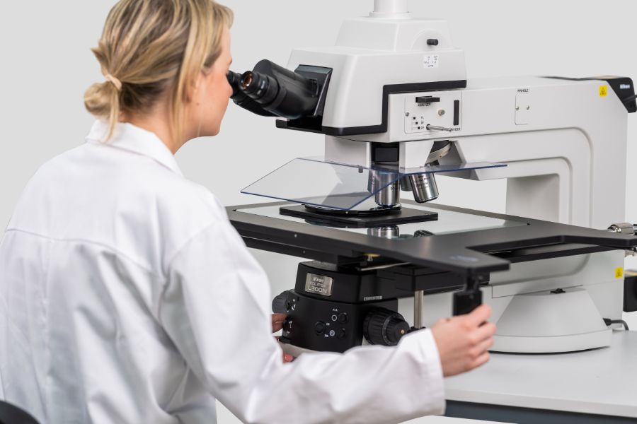
Nikon ECLIPSE L300N(D) and L200N(D)
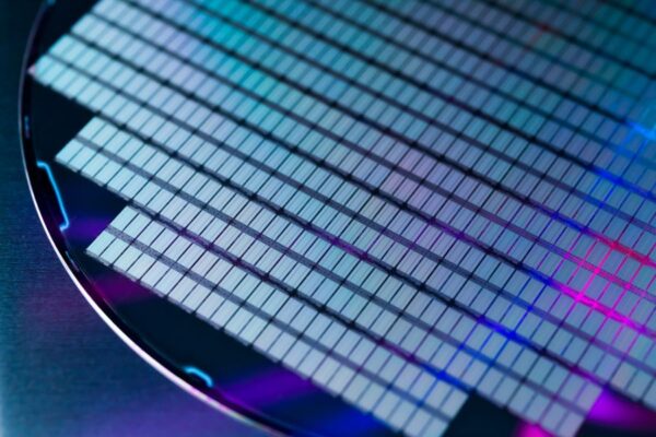
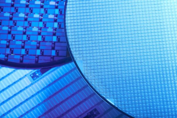
These microscopes are for exceptionally precise optical inspection of wafers (200mm for L200N series and 300mm for L300N series), reticules and other substrates.


ITEMLIST
Products Infomation

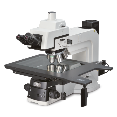
Nikon's ECLIPSE L300ND, L300N and L200ND, L200NA is a range of semiconductor microscopes ideal for inspection of integrated circuits (IC), flat panel displays (FPD), large scale integration (LSI) electronic devices and many more applications.
Industrial Microscopes
Model:
ECLIPSE L300ND, L300N and L200ND, L200N
Maker:
Nikon Metrology NV
These microscopes are for exceptionally precise optical inspection of wafers (200mm for L200N series and 300mm for L300N series), reticules and other substrates.
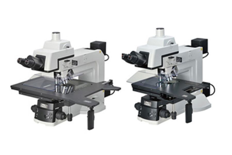
Nikon’s innovative design enables clear imaging techniques, including high contrast, brightfield, darkfield, polarisation (POL), differential interference contrast (DIC) and double beam interferometry optical contrast.
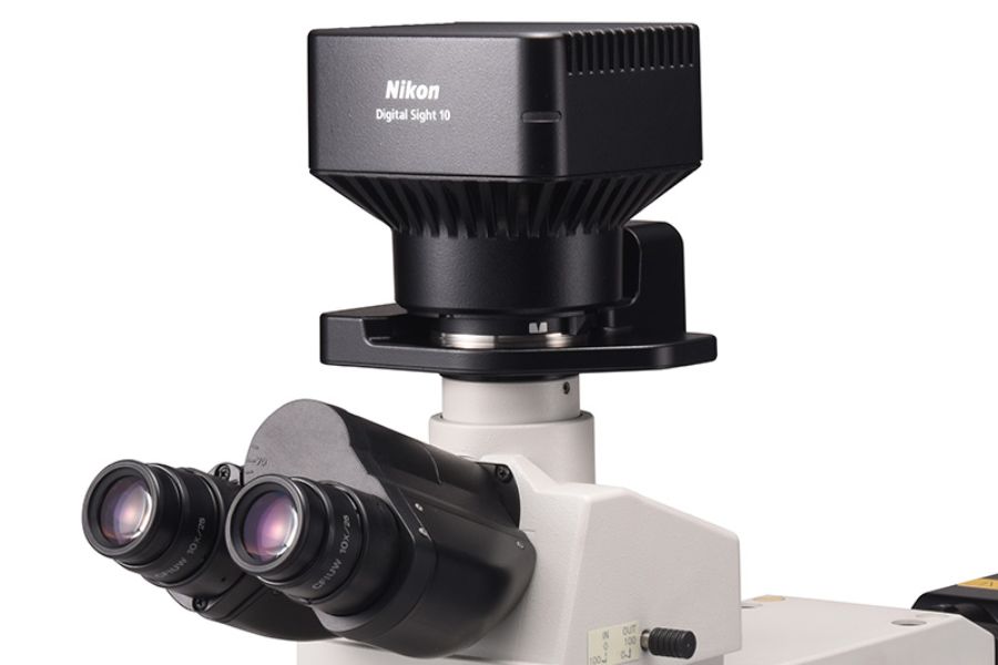
The full range of Nikon’s Digital Sight cameras efficiently captures images of a sample and deliver them to the image processing software of the NIS-Elements suite, together with microscope data on the objective lens used, magnification setting and light intensity.
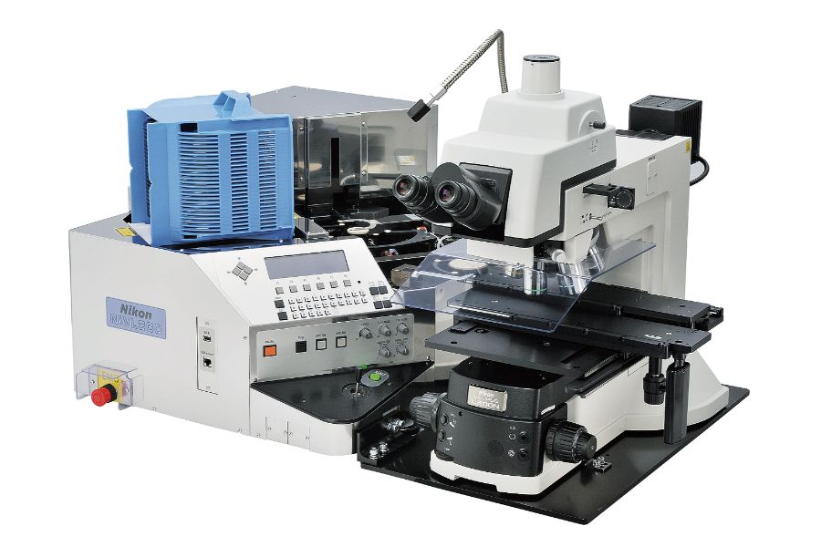
Nikon wafer loaders are well accepted and trusted in the semiconductor industry and many installations are in use today.
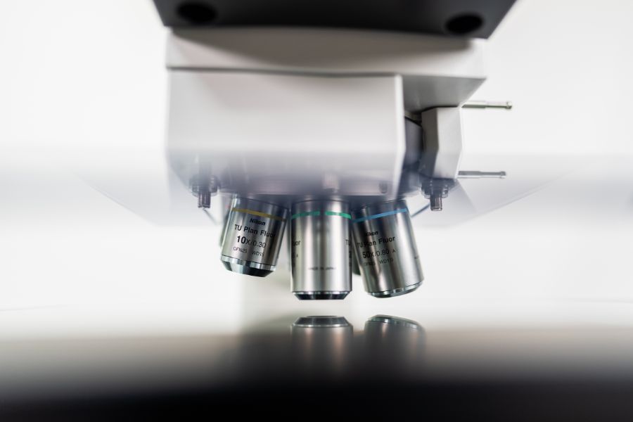
Nikon’s innovative design enables clear imaging techniques, including high-contrast, brightfield, darkfield, polarization (POL), differential interference contrast (DIC) and double beam interferometry optical contrast.
Reflected light: brightfield, darkfield, polarising (POL), differential interference contrast (DIC), epi-fluorescence and two-beam interferometry.
Transmitted light: brightfield, darkfield, polarising, differential interference contrast and phase contrast.
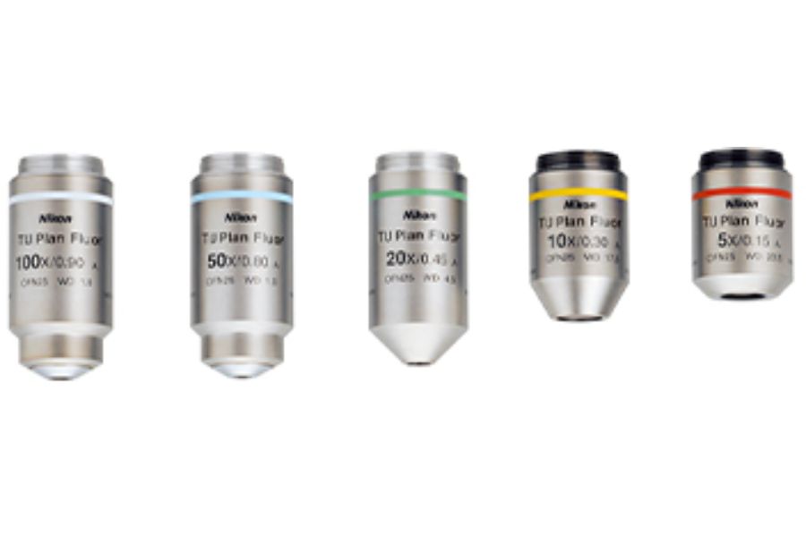
The microscope detects and controls the objective lens in use, light intensity, episcopic illumination and aperture via a USB connection to Nikon’s NIS-Elements software.
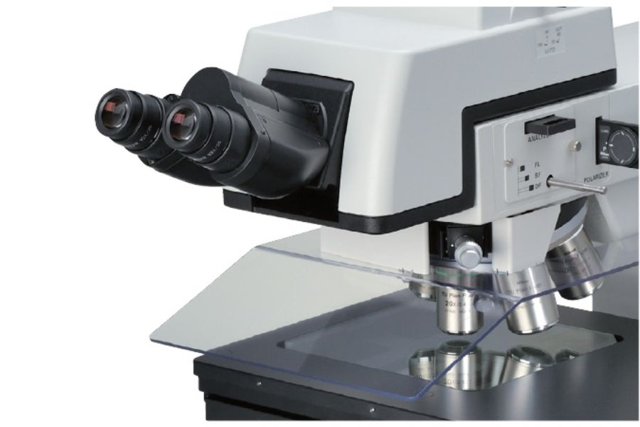
Optimal positioning of operator controls with variable angle eye-tube allows fatigue-free work.
A right-way-up, right-way-around image is provided for correctly observing raw materials, semiconductors and industrial components.


Applications are centred around inspection duties in the electronics and telecommunications sectors.
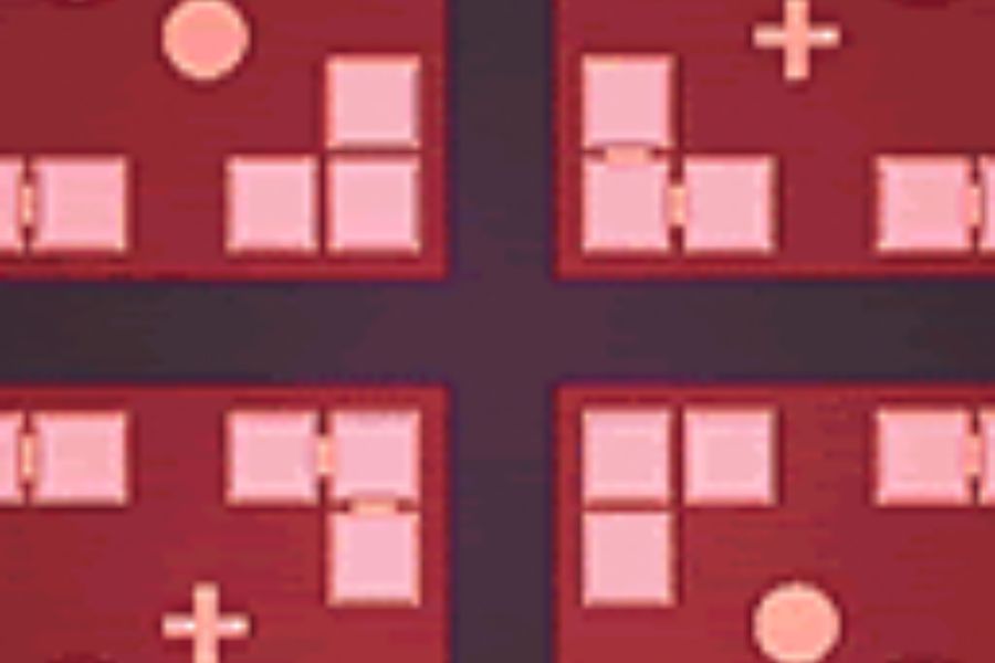
Antennae waveguides are measured with utmost precision, as well as other components such as wafers for semiconductor or photovoltaic devices and micro electro mechanical systems (MEMS) used in smartphones, gyroscopes and accelerometers, for example.
![]()
To view the pdf files, the Adobe Reader from Adobe Systems is required.